Online chat
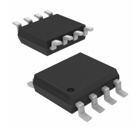
PI6C49CB04BQ2WEX
PI6C49CB04BQ2WEX: Ultra-Low Jitter, Multi-Output Clock Buffer with Fanout & Flexibility
The PI6C49CB04BQ2WEX is a high-performance clock distribution IC manufactured by Pericom Semiconductor (now part of Diodes Incorporated). Designed for applications requiring precise timing synchronization, low jitter, and high reliability, this device is widely used in telecommunications, networking, computing, and industrial systems.
Key Features
- Ultra-Low Jitter Performance
- Additive Phase Jitter (RMS): As low as 50 fs (femtoseconds) (12 kHz to 20 MHz band), ensuring clean clock signals for high-speed data interfaces (e.g., PCIe, SerDes, Ethernet).
- Low Cycle-to-Cycle Jitter: Minimizes timing errors in critical applications like high-frequency trading or 5G base stations.
- Multi-Output Fanout Architecture
- 4 Independent Clock Outputs: Each output can drive multiple loads with minimal skew, ideal for distributing clocks to multiple chips or subsystems.
- Adjustable Output Drive Strength: Supports different load requirements (e.g., LVPECL, LVDS, HCSL, or CMOS levels) via external resistors or internal settings.
- Flexible Input & Output Formats
- Universal Input Support: Accepts differential (LVPECL, LVDS, HCSL) or single-ended (LVCMOS) clock inputs up to 250 MHz.
- Output Format Options: Configurable for LVPECL, LVDS, HCSL, or CMOS to match receiver requirements, reducing external level shifters.
- Low Power & High Efficiency
- Supply Voltage: Operates on 3.3V ±10% (standard) or 2.5V (low-power variants), with typical current consumption of <30 mA.
- Power-Down Mode: Disables outputs to save power when not in use, ideal for battery-operated or energy-sensitive designs.
- Advanced Skew & Phase Control
- Zero-Delay Buffer Mode: Minimizes propagation delay between input and output for deterministic timing.
- Output Skew Matching: Ensures tight phase alignment (<10 ps skew) between outputs for synchronous systems.
- Industrial-Grade Robustness
- Extended Temperature Range: Operates reliably from -40°C to +125°C, suitable for automotive, aerospace, and outdoor deployments.
- ESD Protection: ±2 kV (HBM) on all pins, enhancing reliability in harsh environments.
Applications
- Telecom & Networking:
- 5G base stations, optical transport networks (OTN), and Ethernet switches requiring precise clock distribution.
- Computing & Servers:
- CPU/GPU clock distribution, memory controllers (DDR), and PCIe clocking.
- Industrial Automation:
- PLCs, motion controllers, and robotics with deterministic timing requirements.
- Automotive:
- ADAS, radar systems, and in-vehicle networking (IVN) with automotive-grade temperature support.
- Aerospace & Defense:
- Avionics, radar, and secure communications needing low-jitter, high-reliability clocks.
Advantages
- High Precision, Low Jitter: Critical for maintaining signal integrity in high-speed serial links (e.g., 10G/25G/40G Ethernet, PCIe Gen 5).
- Space-Efficient Design: Compact QFN package reduces PCB footprint in dense systems.
- Flexible I/O Configuration: Eliminates external level shifters and simplifies board design.
- Industrial Temperature Support: Enables deployment in extreme environments without derating.
- Cost-Effective Solution: Replaces multiple discrete clock buffers, lowering BOM costs.
Conclusion
The PI6C49CB04BQ2WEX is a versatile, high-performance clock buffer that combines ultra-low jitter, flexible I/O options, and industrial-grade reliability. Its ability to distribute clean, synchronized clocks across multiple loads makes it ideal for engineers designing timing-critical systems in networking, computing, automotive, and defense applications.
For evaluation, Diodes Incorporated offers development boards, reference designs, and technical support. Contact authorized distributors or visit the Diodes website for product samples, datasheets, and customization options.

DIODES
DIODES
DIODES
DIODES